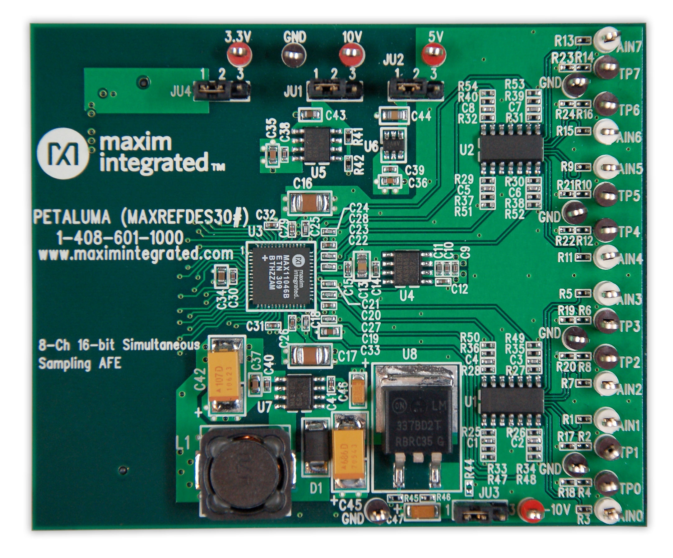
PETALUMA (MAXREFDES30#):8通道同时采样模拟前端
概述
三相功率测量应用要求多路模拟输入,用于测量三相系统中每根线路上的电压和电流。功率监测系统必须同时采样全部模拟输入,以高精度计算瞬时功耗。
Petaluma (MAXREFDES30#)子系统参考设计提供八路高速、250ksps、16位同时采样模拟输入,支持±10V输入信号。
Petaluma设计使用两片四路超高精度、超低噪声输入缓冲器(MAX44252);一片八通道、16位同时采样ADC (MAX11046B);一片超高精度4.096V电压基准(MAX6126);以及+10V、-10V和+5V线性稳压电源(MAX1659, MAX765/LM337、MAX8881)。除三相功率测量应用外,子系统也非常适合于其它任何要求多路同时采样模拟输入的应用,例如多相电机控制和工业振动检测。

详情介绍
Introduction
 More detailed image (JPG) |
Three-phase power measurement applications require multiple analog inputs for voltage and current measurements on each line of the three-phase system. A power monitoring system must sample all of the analog inputs simultaneously to accurately calculate the instantaneous power consumption.
The Petaluma (MAXREFDES30#) subsystem reference design provides eight high-speed, 250ksps, 16-bit simultaneous-sampling analog input channels that accept ±10V input signals.
The Petaluma design utilizes two quadruple ultra-precision, ultra-low-noise input buffers (MAX44252); an 8-channel, 16-bit simultaneous-sampling ADC (MAX11046B); an ultra-high precision 4.096V voltage reference (MAX6126); and regulated +10V, -10V, and +5V power rails (MAX1659, MAX765/LM337, MAX8881). In addition to three-phase power measurement applications, this subsystem also performs well in any application that requires multiple simultaneous sampling of analog inputs, such as multiphase motor control and industrial vibration sensing.

Figure 1. The Petaluma subsystem design block diagram.
Features |
Competitive Advantages |
Applications
|
|
Detailed Description of Hardware
The Petaluma subsystem is optimized for applications that use multiple high-speed, high-accuracy, simultaneous-sampling analog inputs. Figure 1 shows the block diagram of the Petaluma reference design.
The MAX44252 devices (U1 and U2) are quadruple ultra-precision, low-noise op amps. The op amps attenuate and buffer the ±10V input signals to match the input range of the ADC (MAX11046). The MAX44252 devices are set up in the inverting configuration, so the polarity of the signal is reversed at the input of the ADC. The formula to convert the ADC code to voltage is: 10-CODE/65536*20.
The MAX11046 (U3) is a low-cost, 8-channel, 250ksps, 16-bit, single-supply, bipolar, simultaneous-sampling ADC.
Although the MAX11046 ADC has an internal 4.096V voltage reference, Petaluma uses an external MAX6126 (U4) voltage reference to provide the highest possible accuracy. The MAX6126 has an initial accuracy of 0.02% and a 3ppm/°C maximum temperature coefficient (tempco).
By default, the Petaluma is powered from the 12V and 3.3V outputs of the FMC connector on the ZedBoard, if all shunts are installed in the 1–2 position. The MAX1659 (U5) and MAX8881 (U6) provide post-regulated 5V and 10V rails. The MAX765 DC-DC inverter and LM337 negative LDO produce the -10V rail. To use external power supplies, move the shunts on all jumpers to the 2–3 position. Connect the ground terminal of the external power supplies to the GND connector. Connect the 3.3V, 5V, 10V, and -10V supplies to the corresponding connectors on the board.
Petaluma connects to FMC-compatible field-programmable gate array (FPGA)/microcontroller development boards. Petaluma requires supply voltages of 3.3V and 12V from the FMC connector and uses the pin assignments illustrated in Figure 2.

Figure 2. FMC connector pin connections.
Table 1 shows the power requirements. Table 2 shows currently supported platforms and ports.
| Table 1. Power Requirement for the Petaluma Subsystem Reference Design | |||
| Power Type | Jumper Shunt | Input Voltage (V) | Input Current (mA, typ) |
|---|---|---|---|
| On-board power | JU1–JU4: 1–2 | 3.3 | 6.2 |
| 12 | 70 | ||
| External power | JU1–JU4: 2–3 | 3.3 | 6.2 |
| 5 | 41.4 | ||
| 10 | 9.4 | ||
| -10 | 9.4 | ||
| Table 2. Supported Platforms and Ports | ||
| Supported Platforms | Ports | |
|---|---|---|
| ZedBoard platform (Zynq®-7020) | J1 | |
Detailed Description of ZedBoard Firmware
Table 2 shows the currently supported platforms and ports. Support for additional platforms may be added periodically under Firmware Files in the All Design Files section.
The Petaluma firmware released for the ZedBoard kit targets an ARM® Cortex®-A9 processor placed inside a Xilinx Zynq system-on-chip (SoC).
The firmware is a working example of how to interface to the hardware, collect samples, and save them to memory. Figure 3 shows the process flow. The firmware is written in C using the Xilinx SDK tool, which is based on the Eclipse open source standard. Custom Petaluma-specific design functions were created utilizing the AXI MAX11046 custom IP core. The firmware supports the maximum ADC sampling rate at 250ksps.

Figure 3. The Petaluma firmware flowchart.
The firmware accepts commands, configures the ADC, and is capable of downloading blocks of sampled data to a standard terminal program through a virtual COM port. The complete source code is provided to speed up customer development. The corresponding firmware platform files contain code documentation.
Quick Start
Required equipment:
- Windows® PC with two USB ports
- Petaluma (MAXREFDES30#) board
- Petaluma-supported platform (i.e., ZedBoard kit)
- Industrial signal source
Download, read, and carefully follow each step in the appropriate Petaluma (MAXREFDES30#) ZedBoard Quick Start Guide.
Lab Measurements
Equipment used:
- Audio Precision® SYS-2722 signal source or equivalent
- Voltage calibrator DVC-8500
- Windows PC with two USB ports
- Petaluma (MAXREFDES30#) board
- ZedBoard kit
Take special care and use proper equipment when testing the Petaluma design. Duplication of the presented test data requires a signal source with higher accuracy than the design being tested. A low distortion signal source is absolutely required to duplicate the presented results. The input signal was generated using the Audio Precision SYS-2722. The FFTs were created using the FFT control in SignalLab from Mitov Software.
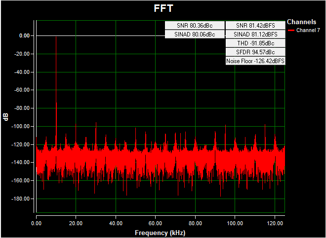
Figure 4. AC FFT for channel 7 (AIN7) using on-board power, a -10V to +10V, 10kHz sine wave input signal, a 250ksps sample rate, and a Blackman-Harris window at room temperature.
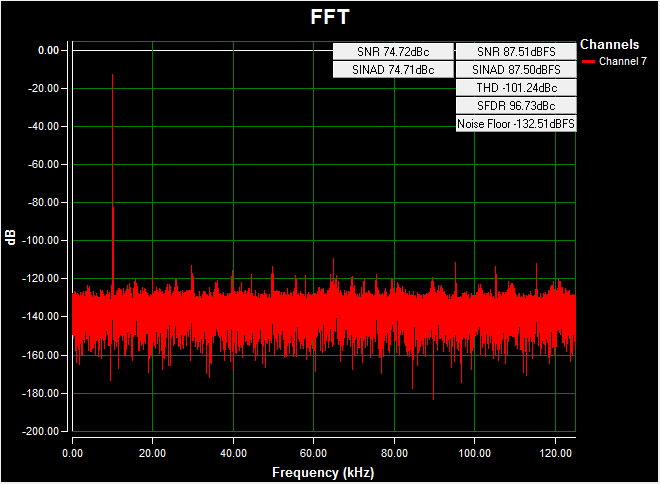
Figure 5. AC FFT for channel 7 (AIN7) using on-board power, a -2.5V to +2.5V, 10kHz sine wave input signal, a 250ksps sample rate, and a Blackman-Harris window at room temperature.
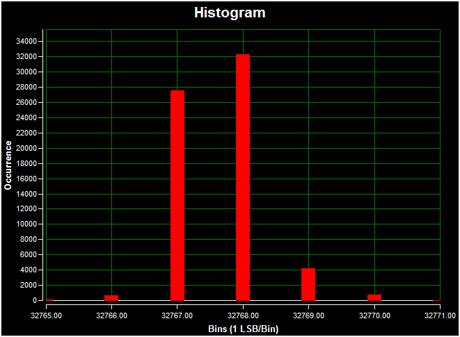
Figure 6. DC histogram for channel 7 (AIN7) using on-board pwer; a 0V DC input signal; a 250ksps sample rate; 65536 samples; a code spread of 21 LSBs with 97.7% of the codes falling within the three center LSBs; and a standard deviation of 0.711 at room temperature.
ARM is a registered trademark and registered service mark of ARM Limited.
Audio Precision is a registered trademark of Audio Precision, Inc.
Cortex is a registered trademark of ARM Limited.
Eclipse is a trademark of Eclipse Foundation, Inc.
Windows is a registered trademark and registered service mark of Microsoft Corporation.
Xilinx is a registered trademark and registered service mark of Xilinx, Inc.
ZedBoard is a trademark of ZedBoard.org.
Zynq is a registered trademark of Xilinx, Inc.