MAXREFDES32#:带反激直流电源的双通道模拟输入/模拟输出

概述
高级制造、定制生产和成本压力持续推动工厂向更高速性能和更高灵活性方向发展。为满足“不妥协”工厂环境的要求,MAXREFDES32#子系统参考设计提供两路高速、高精度、400ksps、16位模拟输入通道和输出通道。所有输入和输出通道支持±10V和±20mA信号,外加20%裕量,为使用电压或电流信号的低、高速系统提供了灵活性。
MAXREFDES32#设计使用四片双通道快速稳定高压运算放大器(MAX9633);两片16位500ksps ADC (MAX11166);两片低噪声、快速稳定、高精度、16位DAC (MAX5316);两片超高精度4.096V电压基准(MAX6126);七片高速数字隔离器(MAX14850);支持反激/Boost电源的峰值电流模式转换器(MAX17498B);以及+18V、-18V、+5V和-1.25V线性稳压电源(MAX8719、MAX8881)。通过使用高精度和高速元件,子系统在过程控制应用(例如传感器输入)和控制应用(例如伺服驱动、分解器和编码器)领域都表现良好。
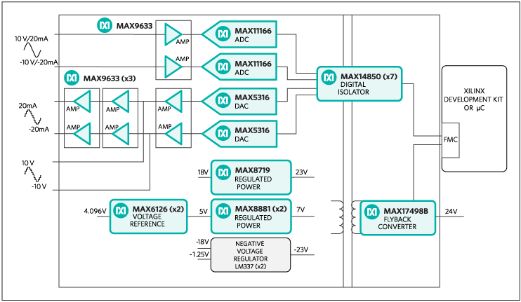
图1. MAXREFDES32子系统设计方框图。
特性
- 两路独立模拟输入
- 两路独立模拟输出
- 隔离电源和数据
- 高速400ksps模拟输入采样率
- 高精度16位分辨率
- 电压输出在17µs内稳定到2 LSB之内
- 电压输出在77µs内稳定到2 LSB之内
- 器件驱动器
- C语言源代码示例
- ZedBoard™平台配置文件
- 兼容FMC
竞争优势
- 高速
- 高精度
- 低噪声
应用
- 工业控制自动化
- 伺服驱动
详情介绍
 放大+
放大+
Introduction
Advanced manufacturing, custom production and cost pressures continue to drive factories to higher speed performance and increased flexibility. To meet the requirements of a ‘no compromises’ factory environment, the MAXREFDES32# subsystem reference design provides two high-speed, high-accuracy, 400ksps, 16-bit analog input channels and output channels. All input and output channels support ±10V and ±20mA signals plus 20% margin, providing flexibility for low- and high-speed systems using either voltage or current signals.
The MAXREFDES32# design utilizes four dual fast-settling high-voltage op amps (MAX9633); two 16-bit 500ksps ADCs (MAX11166); two low-noise, fast-settling precision 16-bit DACs (MAX5316); two ultra-high precision 4.096V voltage references (MAX6126); seven high-speed digital isolators (MAX14850); a peak-current-mode converter for flyback/boost supplies (MAX17498B); and regulated +18V, -18V, +5V, and -1.25V power rails (MAX8719, MAX8881). By using high-accuracy and high-speed components, this subsystem performs well in both process control applications, such as sensor inputs, and control applications, such as servo drives, resolvers, and encoders.
Figure 1. The MAXREFDES32 subsystem design block diagram.
Features
- Two independent analog inputs
- Two independent analog outputs
- Isolated power and data
- High-speed 400ksps analog input sampling rate
- High-accuracy 16-bit resolution
- Voltage output settles to within 2 LSB in 17µs
- Current output settles to within 2 LSB in 77µs
- Device drivers
- Example C source code
- Configuration files for ZedBoard™ platform
- FMC-compatible
Competitive Advantages
- High speed
- High accuracy
- Low noise
Applications
- Industrial control automation
- Servo drive
Detailed Description of Hardware
The MAXREFDES32# subsystem is optimized for applications that need both analog inputs and analog outputs with isolated power and data. Figure 1 shows the block diagram of the MAXREFDES32# reference design.
MAXREFDES32# uses an external MAX6126 (U12 and U22) voltage reference for both the ADC and the DAC to provide the highest possible accuracy. The MAX6126 has an initial accuracy of 0.02% and a 3ppm/ºC maximum temperature coefficient (tempco).
The MAX9633 (U1) is a dual high-voltage, low-noise op amp. The op amps attenuate and buffer the input signals to match the input range of the ADC (MAX11166). When measuring a voltage signal, connect the positive terminal and negative terminal of the signal source to the Vx+/Ix+ and Vx-/Ix- connectors, respectively. When measuring a current signal, connect the positive terminal of the signal source to the Vx+/Ix+ connector, and connect the negative terminal to both Vx-/Ix- and Ix- connectors. The input buffer is configured in a difference amplifier configuration. The equation to convert the ADC code to input voltage is:
V = 3.6621 × 10⁻⁴ × (CODEADC - 32768)
When measuring the current signal, if the Ix- terminal is connected to the ground of the current loop, the equation to convert the ADC code to current is:
I = 7.4466 × 10⁻⁷ × (CODEADC - 32768)
The MAX5316 (U17 and U18) is a low-noise, fast-settling, 16-bit DAC. The range of the DAC outputs is 0V to 4.096V. The dual op amp, MAX9633 (U19), buffers the DAC outputs and rescales the output range to -10V to +10V (±2V) to meet the industrial standard. A second dual op amp, MAX9633 (U20), buffers the outputs of the first MAX9633 (U19). A third dual op amp, MAX9633 (U21), uses the Howland current source configuration to convert the voltage output of the second MAX9633 (U20) into -20mA to +20mA (±4mA) current output. Therefore, the MAXREFDES32# can produce two channels of both voltage and current outputs simultaneously. The equations to convert the DAC code to output voltage and current are:
V = 3.6758 × 10⁻⁴ × CODEDAC - 12.0055
I = 7.3517 × 10⁻⁷ × CODEDAC - 2.4011 × 10⁻²
In standard configuration, the MAXREFDES32# uses the MAX17498B (U23) to generate the isolated +22V, -22V, +7V, and -7V rails from a 24V supply. The MAX8719 (U4), MAX8881 (U5, U6), and LM337 (U7, U8) provide post-regulated +18V, +5V, -18V, and -1.25V rails. Data isolation is accomplished using the MAX14850 (U9–U11, U13–U16) digital data isolators. The combined power and data isolation achieved is 600VRMS. To use external power supplies, disconnect the 24V supply and move the shunts on all jumpers to the 2-3 position. Connect the ground terminal of the external power supplies to the GND connector. Connect the +18V, +5V, -1.25V, and -18V supplies to the corresponding connectors on the board.
MAXREFDES32# connects to FMC-compatible field-programmable gate array (FPGA)/microcontroller development boards. MAXREFDES32# requires a 24V supply and also the 3.3V supply from the FMC connector. The FMC pin assignments are illustrated in Figure 2.

Figure 2. FMC connector pin connections.
Table 1 shows the power requirements. Table 2 shows currently supported platforms and ports.
Table 1. Power Requirement for the MAXREFDES32# Subsystem Reference Design
| Power Type | Jumper Shunt | Input Voltage (V) | Input Current (mA, typ) |
|---|---|---|---|
| MAX17498B Powered | JU1–JU5: 1-2 | 24 | 125 |
| External Power | JU1–JU5: 2-3 | 5 | 88.8 |
| 18 | 26.8 | ||
| -18 | 37.4 | ||
| -1.25 | 1.8 |
Table 2. Supported Platforms and Ports
| Supported Platforms | Ports |
|---|---|
| ZedBoard platform (Zynq®-7020) | J1 |
Detailed Description of ZedBoard Firmware
Table 2 shows the currently supported platforms and ports. Support for additional platforms may be added periodically under Firmware Files in the All Design Files section.
The MAXREFDES32# firmware released for the ZedBoard kit targets an ARM® Cortex®-A9 processor placed inside a Xilinx® Zynq system-on-chip (SoC).
The firmware is a working example of how to interface to the hardware, collect samples, save them to memory, and replicate the input signals on the outputs. Figure 3 shows the process flow. The firmware is written in C using the Xilinx SDK tool, which is based on the Eclipse open source standard. Custom MAXREFDES32# design functions were created utilizing the AXI MAXREFDES32 custom IP core. The firmware supports the maximum ADC sampling rate at 400ksps. The maximum signal replication rate is 60ksps because the settling time for the voltage output signals is 17µs. Because the settling time for current output signals is 77µs, a replication rate of 10ksps or less is recommended.
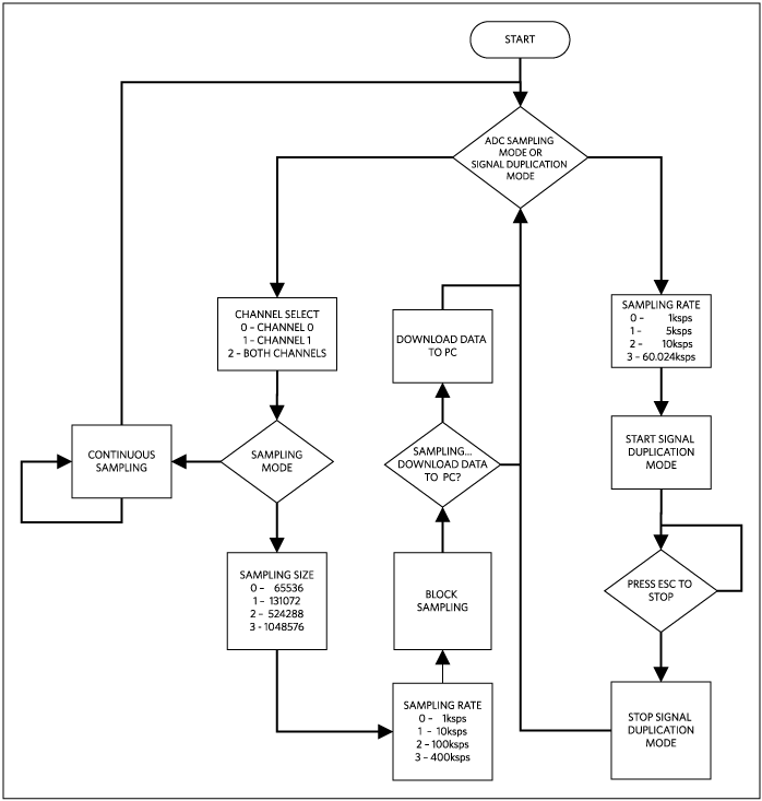
Figure 3. The MAXREFDES32# firmware flowchart.
The firmware accepts commands, configures the ADC and DAC, replicates the inputs on outputs, and is capable of downloading blocks of sampled data to a standard terminal program through a virtual COM port. The complete source code is provided to speed up customer development. The corresponding firmware platform files contain code documentation.
Quick Start
Required Equipment:
- Windows® PC with two USB ports
- MAXREFDES32# (MAXREFDES32#) board
- MAXREFDES32#-supported platform (i.e., ZedBoard kit)
- Industrial signal source
Download, read, and carefully follow each step in the appropriate MAXREFDES32# Quick Start Guide: MAXREFDES32# ZedBoard Quick Start Guide
Lab Measurements
Equipment used for analog input tests:
- Audio Precision® SYS-2722 signal source or equivalent
- Voltage calibrator DVC-8500
- Windows PC with two USB ports
- MAXREFDES32# board
- ZedBoard kit
Equipment used for analog output tests:
- Maxim custom FPGA test board
- One 499Ω, 0.25W resistor load
- Agilent 3458A digital multimeter
- Agilent E3631A DC power supply (any ±24V, 25mA minimum DC power supply works)
- National Instruments GPIB card and cable
- Perl script for controlling the FPGA development kit and measurement equipment
- Windows PC
Take special care and use proper equipment when testing the MAXREFDES32# design. Duplication of the presented test data requires a signal source with higher accuracy than the design being tested. A low distortion signal source is absolutely required to duplicate the presented results. The input signal was generated using the Audio Precision SYS-2722. The FFTs were created using the FFT control in SignalLab from Mitov Software.
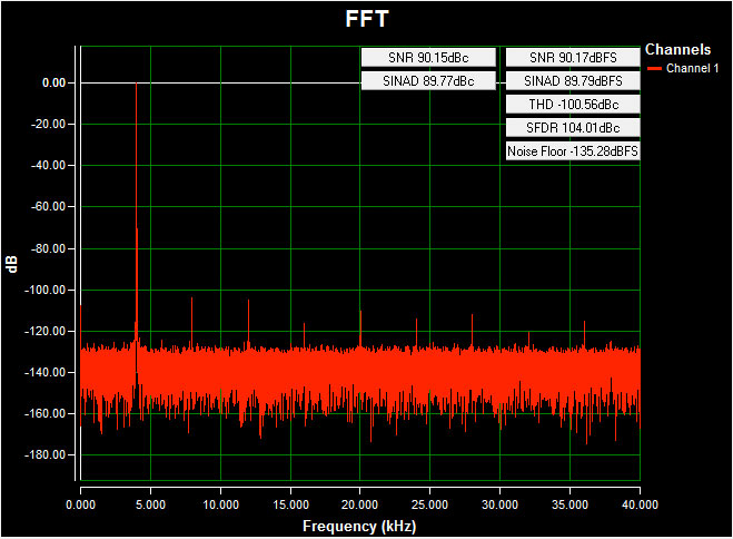
Figure 4. AC FFT for channel 1 (AIN1) using on-board power, a differential -12V to +12V, 20kHz sine wave input signal, a 400ksps sample rate, and a Blackman-Harris window at room temperature.
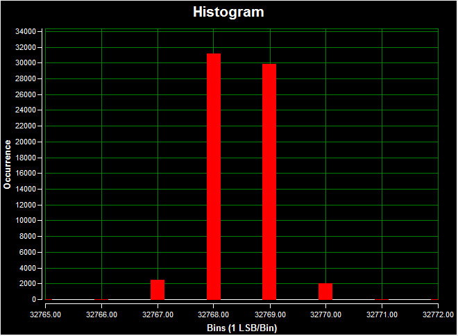
Figure 5. DC histogram for channel 1 (AIN1) using on-board pwer; a 0V DC input signal; a 400ksps sample rate; 65,536 samples; a code spread of 6 LSBs with 99.9% of the codes falling within the four center LSBs; and a standard deviation of 0.625 at room temperature.
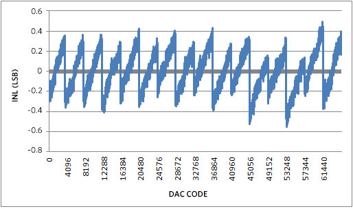
Figure 6. INL for -10V to +10V output range, with 20% overrange.
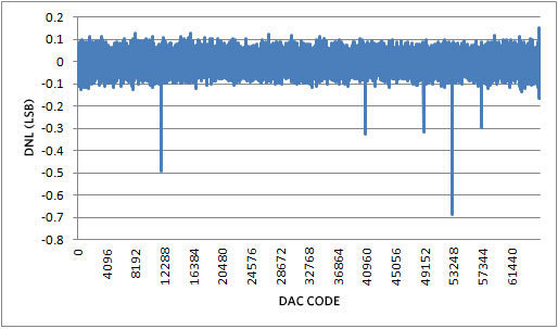
Figure 7. DNL for -10V to +10V output range, with 20% overrange.
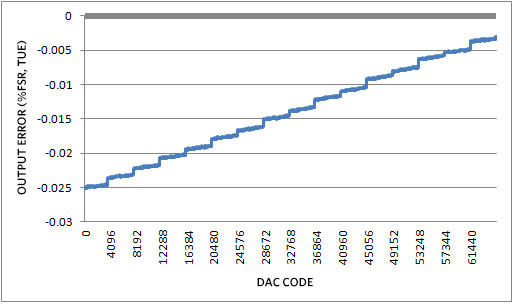
Figure 8. Output error for -10V to +10V output range, with 20% overrange.
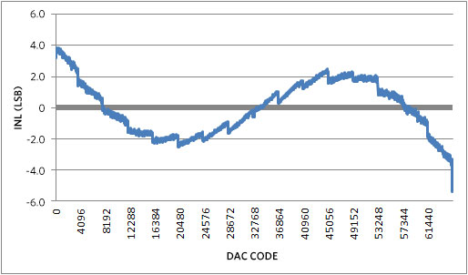
Figure 9. INL for -20mA to +20mA output range, with 20% overrange.
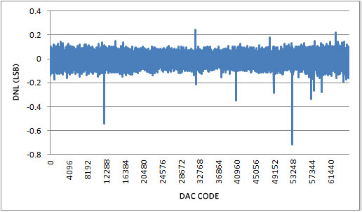
Figure 10. DNL for -20mA to +20mA output range, with 20% overrange.
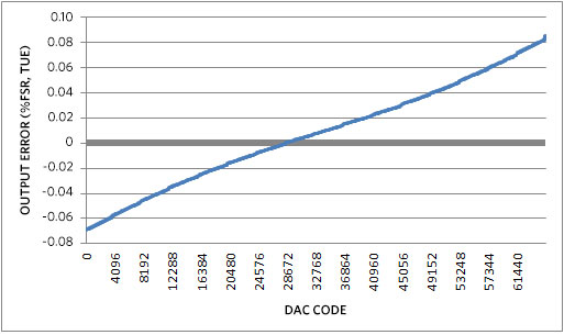
Figure 11. Output error for -20mA to +20mA output range, with 20% overrange.
ARM is a registered trademark and registered service mark of ARM Limited.
Audio Precision is a registered trademark of Audio Precision, Inc.
Cortex is a registered trademark of ARM Limited.
Eclipse is a trademark of Eclipse Foundation, Inc.
Windows is a registered trademark and registered service mark of Microsoft Corporation.
Xilinx is a registered trademark and registered service mark of Xilinx, Inc.
ZedBoard is a trademark of ZedBoard.org
Zynq is a registered trademark of Xilinx, Inc.