MAXREFDES41#:24V至12V、40W隔离电源,带平面变压器
概述
注:该参考设计使用平面变压器。关于使用EFD20磁芯变压器的类似参考设计,请参考MAXREFEDES48#。
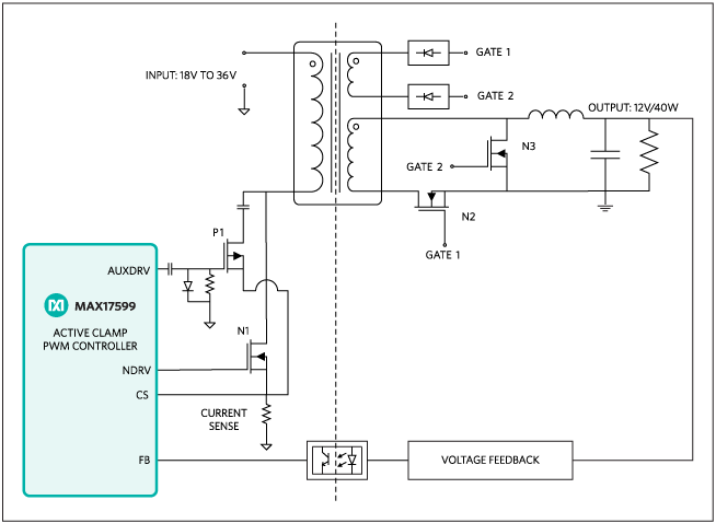
MAXREFDES41#参考设计(图1)演示低IQ、宽输入范围、有源箝位电流模式PWM控制器MAX17599的应用。MAX17599包含设计宽输入、隔离、正激变换器工业电源所需的全部控制电路。参考设计工作在18V至36V输入电压范围,提供高达3.5A @ 12V输出。参考设计具有有源箝位变压器复位结构,适用于正激变换器。该复位结构具有众多优势,包括降低开关上的电压应力、减小变压器尺寸(支持较大的磁通量摆幅)、提高效率(无需有损缓冲电路)。这些特性使其成为结构紧凑、性价比较高的隔离电源。设计的开关频率设置为250kHz。对于EMI敏感应用,用户可设置频率抖动方法,支持低EMI扩频操作。
提供输入欠压锁定(EN/UVLO),用于设置电源启动输入电压(设计中设置为16.5V),以确保掉电条件期间的正确工作。EN/UVLO输入也用于打开/关断IC。提供过压输入(OVI)保护方法,确保控制器在输入电源超过最大允许值(设计中设置为37.0V)时关断。
为控制浪涌电流,器件利用软启动(SS)引脚设置稳压器的软启动时间。通过打嗝过流保护(打嗝模式),将故障条件下的功耗降至最小。器件关断时,软停止提供箝位电容的安全放电,允许控制器以受控方式重新启动。
此外,电流检测电路中提供负电流限制功能,帮助限制动态工作条件下的箝位开关电流。过热故障触发热关断,可靠保护器件。
输入为24V时,参考设计使用提供的元件可实现92.5%的最高效率。该通用电源方案可用于多种不同类型的应用,例如可编程逻辑控制器(PLC)、工业过程控制、工业传感器、电信/数据通信电源、隔离电源充电器、服务器以及嵌入式计算。
系统框图

图1. MAXREFDES41参考设计方框图。
特性
- 功能隔离
- 小巧、灵活
- 低功耗
- 外部元件数量最少
- 在恶劣工业环境下工作可靠
应用
- PLC
- 工业过程控制和传感器
- 电信和数据通信电源
详情介绍
 放大+
放大+
Introduction
Note: This reference design uses a planar transformer. For the similar reference design using an EFD20 core transformer, refer to the MAXREFEDES48#.
The MAXREFDES41# reference design (Figure 1) demonstrates the application of the MAX17599 low IQ, wide-input range, active clamp current-mode PWM controller. The MAX17599 contains all the control circuitry required for the design of wide-input isolated forward-converter industrial power supplies. The reference design operates over an 18V to 36V input voltage range, and provides up to 3.5A at 12V output. The reference design features the active-clamp transformer reset topology for forward converters. This reset topology has several advantages including reduced voltage stress on the switches, transformer size reduction due to larger allowable flux swing, and improved efficiency due to elimination of dissipative snubber circuitry. These features result in a compact and cost-effective isolated power supply. The design is set to switch at 250kHz. For EMI-sensitive applications, the user can program the frequency-dithering scheme, enabling low-EMI spread-spectrum operation.
The input undervoltage lockout (EN/UVLO) is provided for programming the input-supply start voltage (set to 16.5V in the design) and to ensure proper operation during brownout conditions. The EN/UVLO input is also used to turn on/off the IC. The overvoltage input (OVI) protection scheme is provided to make sure that the controller shuts down when the input supply exceeds its maximum allowed value (set to 37.0V in the design).
To control inrush current, the device incorporates a soft-start (SS) pin to set the soft-start time for the regulator. Power dissipation under fault conditions is minimized by hiccup overcurrent protection (hiccup mode). The soft-stop feature provides safe discharging of the clamp capacitor when the device is turned off, and allows the controller to restart in a well-controlled manner.
Additionally, the negative current limit is provided in the current-sense circuitry, helping limit clamp switch current under dynamic operating conditions. An overtemperature fault triggers thermal shutdown for reliable protection of the device.
The reference design delivers a peak efficiency of 92.5% with the supplied components when the input is 24V. This general-purpose power solution can be used in many different types of power applications, such as programmable logic controllers (PLC), industrial process control, industrial sensors, telecom/datacom power supplies, isolated battery chargers, servers, and embedded computing.
System Diagram

Figure 1. The MAXREFDES41 reference design block diagram.
Features
- Functional insulation
- Compact and flexible
- Low power dissipation
- Minimal external components
- Robust operation in adverse industrial environments
Applications
- PLCs
- Industrial process control and sensors
- Telecom and datacom power supplies
Detailed Circuit Description
The MAX17599 low IQ active-clamp current-mode PWM controller contains all the control circuitry required for designing wide-input isolated forward converter industrial power supplies.
The device includes an AUX driver that drives an auxiliary MOSFET (clamp switch) that helps implement the active-clamp transformer reset topology for forward converters. This reset topology has several advantages, including reduced voltage stress on the switches, transformer size reduction due to larger allowable flux swing, and improved efficiency due to elimination of dissipative snubber circuitry. Programmable dead time between the AUX and main driver allows for zero voltage switching.
Primary Power Stage
The active-clamp transformer primary side is driven by an n-channel MOSFET (N1) and a p-channel MOSFET (P1). While N1 is on, power is delivered to the secondary, and magnetizing energy is being stored in the transformer. During this time, P1 is off, and the clamp capacitor (C12) is charged at a constant voltage level.
When N1 turns off, the leakage and magnetizing currents charge up the drain-to-source capacitance of N1. Once the drain-to-source voltage of N1 exceeds the voltage across the clamp capacitor, the body diode of P1 begins to conduct. With the body diode of P1 conducting, the magnetizing current begins to charge the clamp capacitor.
After the body diode of P1 conducts, P1 turns on. This provides zero current switching for the p-channel MOSFET. The clamp capacitor continues to charge until the magnetizing current is reduced to 0A. At this point, the magnetizing current reverses, and the clamp capacitor begins to discharge until the p-channel MOSFET turns off.
After P1 turns off, the clamp capacitor remains at a fixed voltage. There is a fixed delay before N1 turns on. During this delay, the energy in the parasitic components discharges the VDS ofN1 towards VIN. This allows softer turn on and lower switching losses for N1.
The MAX17599 NDRV pin drives the n-channel MOSFET while AUXDRV pin is level shifted through C8, R15, and D3, and then drives the p-channel MOSFET.
Secondary Power Stage
The secondary power stage consists of the synchronous rectifiers (N2, N3), the output filter (L1, C17, C19, C20, and C23), and the gate driving circuit for N2 (R23, Q1, Z1, and R28) and N3 (R24, Q2, Z2, and R29).
When N1 is on, the voltage on the gate wiring of T1 ensures N2 is on, while N3 is off. During this time, a voltage equal to the input voltage multiplied by the NS:NP turns ratio of the transformer is applied across N3; the inductor and the load capacitor are charged and being stored with energy.
When N1 is off, the voltage on the gate wiring of T1 reverses and ensures N2 is off, while N3 is on. During this time, the inductor current flows through N3 and continues transferring energy to the load capacitor.
The voltage on the input end of the filter inductor is a typical buck converter squarewave. The inductor and output capacitors filter the squarewave to produce a DC voltage on the output.
Feedback Control Loop
The feedback network is typical of most isolated forward converters. It is constructed using a TL431V programmable shunt regulator, a 3000V isolation optocoupler, and other RC components.
Startup Voltage and Input Overvoltage Protection Setting (EN/UVLO, OVI)
The EN/UVLO pin in the MAX17599 serves as an enable/disable input, as well as an accurate programmable undervoltage lockout (UVLO) pin. The MAX17599 does not begin startup opera-tions unless the EN/UVLO pin voltage exceeds 1.21V (typ). The MAX17599 turns off if the EN/UVLO pin voltage falls below 1.15V (typ). A resistor divider from the input DC bus to ground can be used to divide down and apply a fraction of the input DC voltage to the EN/ UVLO pin. The values of the resistor divider can be selected so that the EN/UVLO pin voltage exceeds the 1.21V (typ) turn on threshold at the desired input DC bus voltage. The same resistor divider can be modified with an additional resistor, ROVI, to implement overvoltage input protection in addition to the EN/UVLO functionality. When the voltage at the OVI pin exceeds 1.21V (typ), the MAX17599 stops switching. Switching resumes with soft-start operation, only if the voltage at the OVI pin falls below 1.15V (typ). For the expected values of the startup DC input voltage (VSTART) and overvoltage input protection voltage (VOVI), the resistor values for the divider can be calculated as follows:
VSTART = (R6 + R7 + R11)/(R6 + R7) × 1.21 (V)
VOVI = (R6 + R7 + R11)/R6 × 1.21 (V)
If R6 = 24kΩ, R7 = 30kΩ, and R11 = 680kΩ, then:
VSTART = 16.5V, VOVI = 37.0V.
These values give a safe margin for input voltage range of 18V to 36V.
Quick Start
Required equipment:
- MAXREFDES41# board
- One adjustable DC power supply with a voltage output up to 37V and current up to 3A.
- One electronic load
- 2 voltmeters
- 2 ammeters
Procedure
The MAXREFDES41# board is fully assembled and tested. Use the following steps to verify board operation.
- Turn off the power supply.
- Connect the positive terminal of the power supply to the VIN connector of the MAXREFDES41# board.
- Connect the PGND connector of the MAXREFDES41# board to the positive terminal of one ammeter. Connect the negative terminal of the ammeter to the negative terminal of the power supply.
- Connect one voltmeter across the VIN and the PGND connectors of the MAXREFDES41# board.
- Connect the VOUT connector of the MAXREFDES41# board to the positive terminal of the electronic load.
- Connect the negative terminal of the electronic load to the positive terminal of the second ammeter. Connect the negative terminal of the ammeter to the GNDO connector of the MAXREFDES41# board.
- Connect the second voltmeter across the VOUT and the GNDO connectors of the MAXREFDES41# board.
- Turn on the power supply. Set the output to 24V.
- Set the electronic load to a constant current between 0A to 3.5A.
- Verify the second voltmeter reading is 12V ±0.12V.
Lab Measurements
The MAXREFDES41# design was verified and tested under full input range and different output load conditions.
The power efficiency vs. load current is illustrated in Figure 2.

Figure 2. Power efficiency vs. load current.
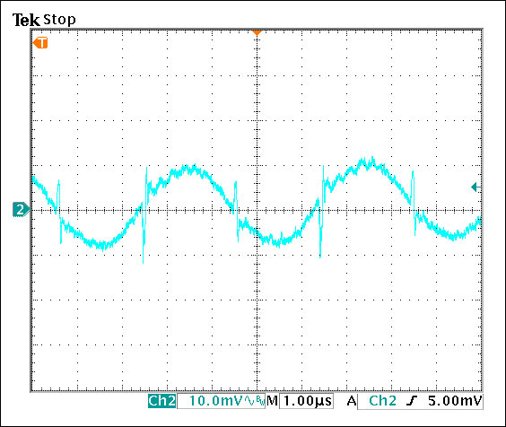
Figure 3 display the output ripple at full load (ripple + spike is 20mVP-P) when the input is 24V.

Figure 3. Output ripple at 3.5A load.
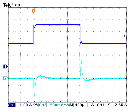
Figure 4 displays the load transient response when the load is stepped from 5mA to 400mA, and then dropped back to 5mA again.The output transient spike is about 240mV. The input is 24V.

Figure 4. Transient response when load steps from 5mA to 400mA.
Figure 5 shows the load transient response when the load is stepped from 2A to 3.5A, and then dropped back to 2A again.The transient voltage is about 800mV. The input is 24V.

Figure 5. Transient response when load steps from 2A to 3.5A.

