MAXREFDES121#: Isolated 24V to 3.3V 33W Power Supply
Maxim的电源专家设计和建造了一系列隔离型工业电源参考设计,其中每款电源将24V高效转换为各种功率水平的电压轨。每种电源轨都采用商用变压器进行隔离,有助于快速、便捷地选择变压器。每款设计均经过负载及电源调整率测试,以及效率和瞬态性能测试。
备有经过空间优化的电路板可供购买。每块电路板都具有高电流引脚,设计用于安装在PCB上,就像一个模块,进一步加速开发和生产。所有的Maxim参考设计均提供BOM、原理图、布局文件以及Gerber文件。
特性
- 功能隔离
- 小巧、灵活
- 低功耗
- 外部元件数量最少
- 在恶劣工业环境下工作可靠
应用
- PLCs
- 工业过程控制和传感器
- 电信和数据通信电源
详情介绍
Introduction
MAXREFDES121# is an efficient active-clamp topology design with 24V input, and a 3.3V output at 33W of power (10A). The design (Figure 1) demonstrates the application of the MAX17599 low IQ, wide-input range, active clamp current-mode PWM controller. This entire design fits on a 70mm x 20mm circuit board.
The MAX17599 contains all the control circuitry required for the design of wide-input isolated forward-converter industrial power supplies. The reference design operates over an 18V to 36V input-voltage range, and provides up to 10A at 3.3V output. The reference design features the active-clamp transformer reset topology for forward converters. This reset topology has several advantages including reduced voltage stress on the switches, transformer-size reduction due to larger allowable flux swing, and improved efficiency due to elimination of dissipative snubber circuitry. These features result in a compact and cost-effective isolated power supply. The design is set to switch at 250kHz. For EMI-sensitive applications, the user can program the frequency-dithering scheme, enabling low-EMI spread-spectrum operation.
The input undervoltage lockout (EN/UVLO) is provided for programming the input-supply start voltage (set to 18V in the design) and to ensure proper operation during brownout conditions. The EN/UVLO input is also used to turn on/off the IC. The overvoltage input (OVI) protection scheme is provided to make sure that the controller shuts down when the input supply exceeds its maximum allowed value (set to 36V in the design).
To control inrush current, the device incorporates a soft-start (SS) pin to set the soft-start time for the regulator. Power dissipation under fault conditions is minimized by hiccup overcurrent protection (hiccup mode). The soft-stop feature provides safe discharging of the clamp capacitor when the device is turned off, and allows the controller to restart in a well-controlled manner.
Additionally, the negative current limit is provided in the current-sense circuitry, helping limit clamp switch current under dynamic operating conditions. An overtemperature protection (OTP) fault triggers thermal shutdown for reliable protection of the device.
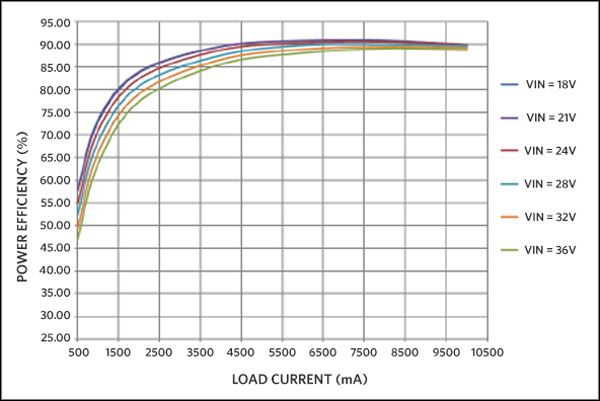
The reference design delivers a peak efficiency of 90.82% with the supplied components when the input is 24V. This general-purpose power solution can be used in many different types of power applications, such as programmable logic controllers (PLC), industrial process control, industrial sensors, telecom/datacom power supplies, isolated battery chargers, servers, and embedded computing.
System Diagram
 Figure 1. The MAXREFDES121# reference design block diagram.
Detailed Circuit Description
The MAX17599 low IQ active-clamp current-mode PWM controller contains all the control circuitry required for designing wide-input isolated forward converter industrial power supplies.
The device includes an AUX driver that drives an auxiliary MOSFET (clamp switch) that helps implement the active-clamp transformer reset topology for forward converters. This reset topology has several advantages, including reduced voltage stress on the switches, transformer-size reduction due to larger allowable flux swing, and improved efficiency due to elimination of dissipative snubber circuitry. Programmable dead time between the AUX and main driver allows for zero voltage switching.
Primary Power Stage
The active-clamp transformer primary side is driven by an n-channel MOSFET (N3) and a p-channel MOSFET (P1). While N3 is on, power is delivered to the secondary side, and magnetizing energy is being stored in the transformer. During this time, P1 is off, and the clamp capacitor (C10) is charged at a constant voltage level.
When N3 turns off, the leakage and magnetizing currents charge up the drain-to-source capacitance of N3. Once the drain-to-source voltage of N3 exceeds the voltage across the clamp capacitor, the body diode of P1 begins to conduct. With the body diode of P1 conducting, the magnetizing current begins to charge the clamp capacitor.
After the body diode of P1 conducts, P1 turns on. This provides zero current switching for the p-channel MOSFET. The clamp capacitor continues to charge until the magnetizing current is reduced to 0A. At this point, the magnetizing current reverses, and the clamp capacitor begins to discharge until the p-channel MOSFET turns off.
After P1 turns off, the clamp capacitor remains at a fixed voltage. There is a fixed delay before N3 turns on. During this delay, the energy in the parasitic components discharges the VDS of N3 towards VIN. This allows softer turnon and lower switching losses for N3.
The MAX17599 NDRV pin drives the n-channel MOSFET while the AUXDRV pin is level shifted through C11, R9, R14, and D4, and then drives the p-channel MOSFET.
Secondary Power Stage
The secondary power stage consists of the synchronous rectifiers (N1, N2), the output filter (L1, C4, C5, and C6), and the gate driving circuit for N1 (R3) and N2 (R2).
When N3 is on, the voltage on the gate wiring of T1 ensures N2 is on, while N1 is off. During this time, a voltage equal to the input voltage multiplied by the NS:NP turns ratio of the transformer is applied across N3; the inductor and the load capacitor are charged and being stored with energy.
When N3 is off, the voltage on the gate wiring of T1 reverses and ensures N2 is off, while N1 is on. During this time, the inductor current flows through N1 and continues transferring energy to the load capacitor.
The voltage on the input end of the filter inductor is a typical buck-converter square wave. The inductor and output capacitors filter the square wave to produce DC voltage on the output.
Feedback Control Loop
A feedback network is typical of most isolated forward converters. It is constructed using a TL431V programmable shunt regulator, a 3000V isolation optocoupler, and other RC components.
Startup Voltage and Input Overvoltage Protection Setting (EN/UVLO and OVI pins)
The EN/UVLO pin in the MAX17599 serves as an enable/disable input, as well as an accurate programmable undervoltage lockout (UVLO) pin. The MAX17599 does not begin startup opera-tions unless the EN/UVLO-pin voltage exceeds 1.21V (typ). The MAX17599 turns off if the EN/UVLO pin voltage falls below 1.15V (typ). A resistor divider from the input DC bus to ground can be used to divide down and apply a fraction of the input DC voltage to the EN/ UVLO pin. The values of the resistor-divider can be selected so that the EN/UVLO-pin voltage exceeds the 1.21V (typ) turnon threshold at the desired input DC bus voltage. The same resistor-divider can be modified with an additional resistor, ROVI, to implement overvoltage input protection in addition to the EN/UVLO functionality. When the voltage at the OVI pin exceeds 1.21V (typ), the MAX17599 stops switching. Switching resumes with soft-start operation, only if the voltage at the OVI pin falls below 1.15V (typ). For the expected values of the startup DC input voltage (VSTART) and overvoltage input protection voltage (VOVI), the resistor values for the divider can be calculated as follows:
VSTART = (R4 + R7 + R5)/(R4 + R7) × 1.21 (V)
VOVI = (R4 + R7 + R5)/R4 × 1.21 (V)
If R4 = 24.9kΩ, R5 = 698kΩ, and R7 = 24.9kΩ, then:
VSTART = 18.2V, VOVI = 36.3V.
Quick Start
Required equipment:
- MAXREFDES121# board
- One adjustable DC power supply with a voltage output up to 37V and current up to 3A.
- One electronic load
- 2 voltmeters
- 2 ammeters
Procedure
The MAXREFDES121# board is fully assembled and tested. Use the following steps below to verify board operation.
- Turn off the power supply.
- Connect the positive terminal of the power supply to the VIN connector of the MAXREFDES121# board.
- Connect the PGND connector of the MAXREFDES121# board to the positive terminal of one ammeter.
- Connect the negative terminal of the ammeter to the negative terminal of the power supply.
- Connect one voltmeter across the VIN and the PGND connectors of the MAXREFDES121# board.
- Connect the VOUT connector of the MAXREFDES121# board to the positive terminal of the electronic load.
- Connect the negative terminal of the electronic load to the positive terminal of the second ammeter.
- Connect the negative terminal of the ammeter to the GNDO connector of the MAXREFDES121# board.
- Connect the second voltmeter across the VOUT and the GNDO connectors of the MAXREFDES121# board.
- Turn on the power supply. Set the output to 24V.
- Set the electronic load to a constant current between 0A to 10A.
- Verify the second voltmeter reading is 3.3V (±0.15V).
Lab Measurements
The MAXREFDES121# design was verified and tested under full input range and different output load conditions.
The power efficiency vs. load current is illustrated in Figure 2.
 Figure 2. Power efficiency vs. load current.
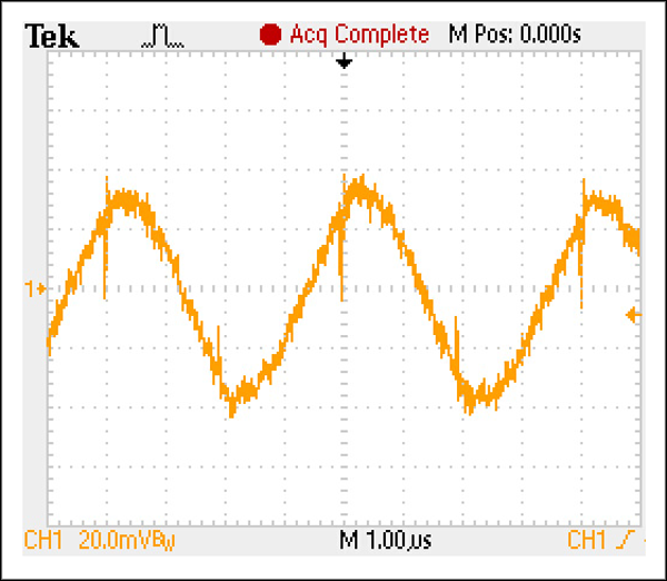
Figure 3 display the output ripple at full load (ripple + spike is ±40mV) when the input is 24V.
 Figure 3. Output ripple at 10A load.
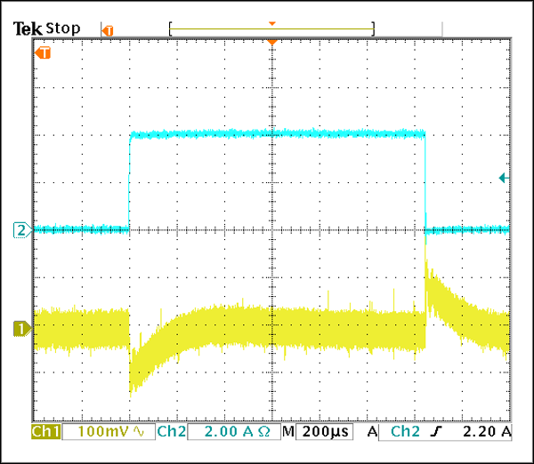
Figure 4 displays the load transient response when the load is stepped from 5mA to 4A, and then dropped back to 5mA again.The output transient spike is about 120mV. The input is 24V.
 Figure 4. Transient response when load steps from 5mA to 4A.
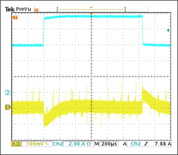
Figure 5 shows the load transient response when the load is stepped from 6A to 10A, and then dropped back to 6A again.The transient voltage is about 120mV. The input is 24V.
 Figure 5. Transient response when load steps from 6A to 10A.


