MAXREFDES125#: Non-isolated 24V to 5.1V, 20W Power Supply
MAXREFDES125#为高效、20W电源,适合工业和各种电源应用。突破性的设计实现了96%以上的效率,具有17V至36V较宽输入电压范围。系统提供5.1V @ 4A输出电压轨,满足众多大功耗系统的需求。系统的核心是MAX17536同步降压型转换器。MAX17536 能够工作在多种模式,无需肖特基二极管即可同步操作,以及内部补偿和内置软启动。所以能够实现适合任何系统的小尺寸、超高效率电源。
MAXREFDES125#电路板的面积为20mm x 35mm。网站提供全部设计文件,备有电路板可供购买。
特性
- 高效率
- 小巧、灵活
- 低功耗
- 外部元件数量最少
- 在恶劣工业环境下工作可靠
应用
- PLC
- 工业过程控制和传感器
- 电信和数据通信电源
详情介绍
Introduction
The MAXREFDES125# reference design (Figure 1) demonstrates the application of the MAX17536 high-efficiency, high-voltage, synchronous step-down controller. The MAX17536 can be operated in the pulse-width modulation (PWM), pulse-frequency modulation (PFM), or discontinuous-conduction mode (DCM) control schemes. The reference design operates over a 17V to 36V input-voltage range, and provides up to 4A at 5.1V output. The reference design features high-efficiency, multiple mode, synchronous buck topology for step-down converters. In PWM mode, the inductor current is allowed to go negative, PWM operation provides constant frequency opera-tion at all loads, and is useful in applications sensitive to switching frequency. PFM mode of operation disables negative inductor current and additionally skips pulses at light loads for high efficiency. DCM mode of operation features constant-frequency operation down to lighter loads than PFM mode by not skipping pulses and only disabling negative inductor current at light loads. DCM operation offers efficiency performance that lies between PWM and PFM modes. The reference design features pins beneath the board to enable the board to be designed into a larger system, as a module. Pins are 15.24mm (0.6in) from power to ground, and 27.94mm (1.1in) from the input side to the output side.
The input undervoltage lockout (EN/UVLO) is provided for programming the input-supply start voltage (set to 14.5V in the design) and to ensure proper operation during brownout conditions. The EN/UVLO input is also used to turn on/off the IC.
To control inrush current, the device incorporates a soft-start (SS) pin to set the soft-start time for the regulator. Power dissipation under fault conditions is minimized by hiccup-overcurrent protection (hiccup mode).
The reference design delivers a peak efficiency of 96.5% with the supplied components when the input is 24V. This general-purpose power solution can be used in many different types of power applications, such as industrial PLCs, actuators and sensors.
System Diagram
 Figure 1. The MAXREFDES125# reference design block diagram.
Detailed Circuit Description
Hardware Description
The MAX17536 high-efficiency, high-voltage, synchronous step-down DC-DC converter with integrated high-side MOSFET operates over a 4.5V to 60V input. The converter delivers up to 4A and generates output voltages from 0.9V up to 0.9 × VIN.
The MAX17536 uses peak current-mode control. The device may be operated in the pulse-width modulation (PWM), pulse-frequency modulation (PFM), and discontinuous-conduction mode (DCM) control schemes.
Mode Selection
The logic state of the MODE/SYNC pin is latched when VCC and EN/UVLO voltages exceed the respective UVLO rising thresholds and all internal voltages are ready to allow LX switching. If the MODE/SYNC pin is open at power-up, the device operates in PFM mode at light loads. If the MODE/SYNC pin is grounded at power-up, the device operates in constant-frequency PWM mode at all loads. Finally, if the MODE/SYNC pin is connected to VCC at power-up, the device operates in constant-frequency DCM mode at light loads. State changes on the MODE/SYNC pin are ignored during normal operation.
In PWM mode, the inductor current is allowed to go negative. PWM operation provides constant frequency operation at all loads, and is useful in applications sensitive to switching frequency. However, the PWM mode of operation gives lower efficiency at light loads compared to PFM and DCM modes of operation.
PFM mode of operation disables negative inductor current and additionally skips pulses at light loads for high efficiency. In PFM mode, the inductor current is forced to a fixed peak of 2A every clock cycle until the output rises to 102.3% of the nominal voltage. Once the output reaches 102.3% of the nominal voltage, both the high-side and low-side FETs are turned off and the device enters hibernate operation until the load discharges the output to 101.1% of the nominal voltage. Most of the internal blocks are turned off in hibernate operation to save quiescent current. After the output falls below 101.1% of the nominal voltage, the device comes out of hibernation, turns on all internal blocks, and again commences the process of delivering pulses of energy to the output until it reaches 102.3% of the nominal output voltage. The advantage of the PFM mode is higher efficiency at light loads because of lower quiescent current drawn from the supply. The disadvantage is that the output-voltage ripple is higher compared to PWM or DCM modes of operation and switching frequency is not constant at light loads.
DCM mode of operation features constant-frequency operation down to lighter loads than PFM mode, by not skipping pulses but only disabling negative inductor current at light loads. DCM operation offers efficiency performance that lies between PWM and PFM modes.
Table 1 shows Reference Design jumper (JU1) settings that can be used to configure the desired mode of operation.
Table 1. MODE Description (JU1)
| Shunt Position | EN/UVLO Pin | MAX17536 Mode |
|---|---|---|
| 1-2* | Connected to SGND | PWM mode of operation |
| Not installed | Unconnected | PWM mode of operation |
| 2-3 | Connected to VCC | DCM mode of operation |
*Default position.
Linear Regulator (VCC and EXTVCC)
The device has two internal low-dropout (LDO) regulators which power VCC. One LDO is powered from VIN (IN LDO) and the other LDO is powered from EXTVCC (EXTVCC LDO). Only one of the two LDOs is in operation at any given time, depending on the voltage levels present at EXTVCC. If the EXTVCC voltage is greater than 4.7V (typ), VCC is powered from EXTVCC. If EXTVCC is lower than 4.7V (typ), VCC is powered from VIN. Powering VCC from EXTVCC increases efficiency at higher input voltages. EXTVCC voltage should not exceed 24V.
Loop Compensation
The MAX17536 is internally loop compensated. However, if the switching frequency is less than 450kHz, connect a 0402 capacitor (C10) between the CF pin and the FB pin to keep the compensation loop stable.
Input Undervoltage-Lockout Level Setting (EN/UVLO)
The MAX17536 offers an adjustable input undervoltage-lockout level. Set the voltage level with a resistive voltage-divider connected from VIN to SGND. Connect the center node of the divider to EN/UVLO.
Choose R1 to be 3.32M and then calculate R2 as follows:

where VINU is the voltage required to turn on the device. The VINU in this design is 14.5V.
For normal operation, a shunt should be installed across pins 1-2 on JU2. To disable the output, install a shunt across pins 2-3 on JU2 and pull the EN/UVLO pin to GND. See Table 2 for JU2 settings.
Table 2. Regulator Enable (EN/UVLO) Description (JU2)
| Shunt Position | EN/UVLO Pin | MAX17536 Output |
|---|---|---|
| 1-2* | Connected to VIN | Enabled |
| Not installed | Connected to the center node of resistor-divider R1 and R2 | Enabled, UVLO level set through the R1 and R2 resistors |
| 2-3 | Connected to SGND | Disabled |
*Default position.
Quick Start Guide
Required Equipment:
- MAXREFDES125#
- One adjustable DC power supply with voltage output up to 36V and current up to 2A
- One electronic load
- Two voltmeters
- Two ammeters
Procedure
The MAXREFDES125# board is fully assembled and tested. Use the following steps to verify board operation.
- Turn off the power supply.
- Connect the positive terminal of the power supply to the VIN connector of the MAXREFDES125# board.
- Connect the PGND connector of the MAXREFDES125# board to the positive terminal of one ammeter. Connect the negative terminal of the ammeter to the negative terminal of the power supply.
- Connect one voltmeter across the VIN and the PGND connectors of the MAXREFDES125# board.
- Connect the VOUT connector of the MAXREFDES125# board to the positive terminal of the electronic load.
- Connect the negative terminal of the electronic load to the positive terminal of the second ammeter. Connect the negative terminal of the ammeter to the GNDO connector of the MAXREFDES125# board.
- Connect the second voltmeter across the VOUT and the GNDO connectors of the MAXREFDES125# board.
- Verify that shunt is installed across pins 1-2 on jumper JU1.
- Verify that shunt is installed across pins 1-2 on jumper JU2.
- Turn on the power supply. Set the output to 24V.
- Set the electronic load to a constant current between 0A to 4A.
- Verify the second voltmeter reading is 5.1V ±0.255V.
Lab Measurements
The MAXREFDES125# was verified and tested under full input range and different output load conditions. The power efficiency vs. load current, PWM MODE, is illustrated in Figure 2.
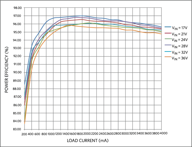 Figure 2. Power efficiency vs. load current, PWM MODE.
The power efficiency vs. load current, PFM MODE, is illustrated in Figure 3. Note that the x-axis is logarithmic in Figure 3 and Figure 4.
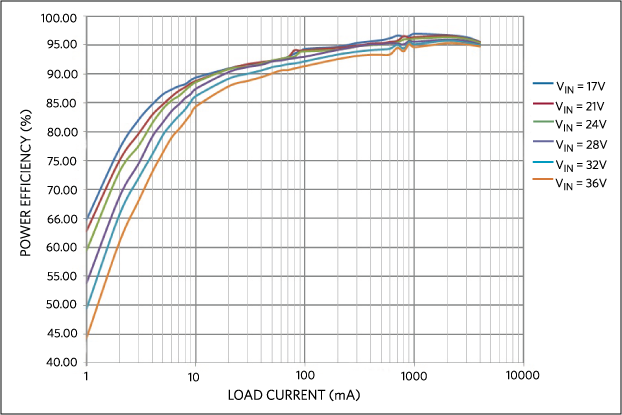 Figure 3. Power efficiency vs. load current, PFM MODE.
The power efficiency vs. load current, DCM MODE, is illustrated in Figure 4.
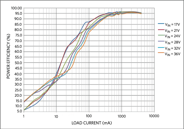 Figure 4. Power efficiency vs. load current, DCM MODE.
Figure 5 displays the output ripple at full load when the input is 24V.
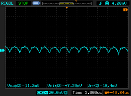 Figure 5. Output ripple at 4A load.
Figure 6 displays the load transient response when the load is stepped from 200mA to 2A, and then dropped back to 200mA again in PWM MODE. The input is 24V.
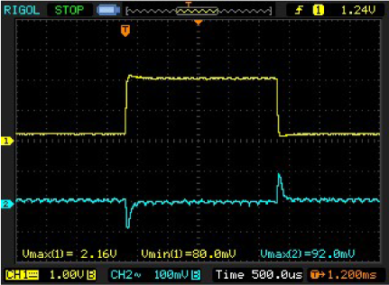 Figure 6. Transient response when load steps from 200mA to 2A in PWM MODE.
Figure 7 displays the load transient response when the load is stepped from 2A to 4A, and then dropped back to 2A again in PWM MODE. The input is 24V.
 Figure 7. Transient response when load steps from 2A to 4A in PWM MODE.
Figure 8 displays the load transient response when the load is stepped from 200mA to 2A, and then dropped back to 200mA again in PFM MODE. The input is 24V.
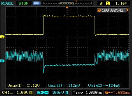 Figure 8. Transient response when load steps from 200mA to 2A in PFM MODE.
Figure 9 displays the load transient response when the load is stepped from 2A to 4A, and then dropped back to 2A again in PFM MODE. The input is 24V.
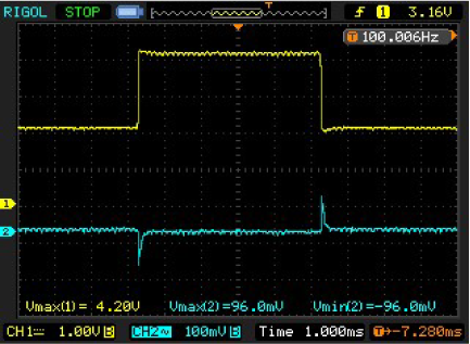 Figure 9. Transient response when load steps from 2A to 4A in PFM MODE.
Figure 10 displays the load transient response when the load is stepped from 200mA to 2A, and then dropped back to 200mA again in DCM MODE. The input is 24V.
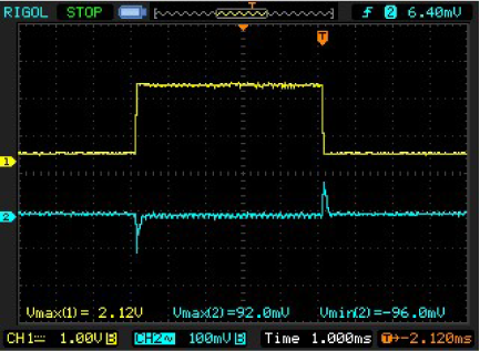 Figure 10. Transient response when load steps from 200mA to 2A in DCM MODE.
Figure 11 displays the load transient response when the load is stepped from 2A to 4A, and then dropped back to 2A again in DCM MODE. The input is 24V.
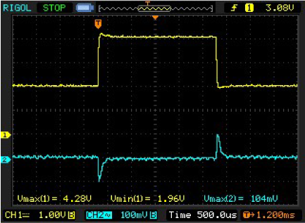 Figure 11. Transient response when load steps from 2A to 4A in DCM MODE.


