3.3V to 40V Low Noise APD Bias Power Supply
详情介绍


概览
设计资源
设计集成文件
• Schematic• Bill of Materials
• Gerber Files
• Layout Files (PADs)
• Assembly Drawing 下载设计文件 1.54 M
评估硬件
产品型号带"Z"表示符合RoHS标准。评估此电路需要下列选中的电路板
- ADL5801-EVALZ ($140.00) ADL5801-EVALZ
- EV-ADF4355-2SD1Z ($300.00) EV-ADF4355-2SD1Z
- EVAL-CN0369SDPZ ($300.00) EVAL-CN0369SDPZ
- EVAL-SDP-CS1Z ($49.00) Eval Control Board
优势和特点
- Translation Loop Synthesizer
- 5GHz to 5.4GHz RF Output
- Low Phase Noise
电路功能与优势
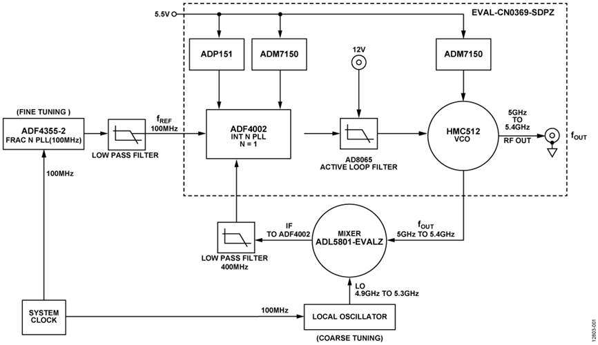
The circuit block diagram shown in Figure 1 is a low phase noise translation loop synthesizer (also known as an offset loop). This circuit translates the lower 100 MHz reference frequency of the
ADF4002 phase locked loop (PLL) up to a higher frequency range of 5.0 GHz to 5.4 GHz, as determined by the frequency of the local oscillator (LO).

The translation loop synthesizer has very low phase noise (<50 fs) in contrast to a synthesizer using only a PLL. The low phase noise is because of the very low N value used by the ADF4002 integer-N PLL, which controls the voltage controlled oscillator (VCO). In this example, the ADF4002 phase frequency detector (PFD) runs at 100 MHz, and N = 1, yielding phase noise performance that is not limited by the N value of the PLL.
电路描述
The PLL noise floor, PNTOT1, is given by
where:
PNSYNTH is the synthesizer FOM and is device specific.
N is the divider used by the PLL.
fPFD is the frequency of the phase frequency detector.
A PLL whose N value = 1 has a noise floor of 10log 10(f PFD).
The PLL 1/f noise, PN TOT2, is given by
where:
PN1/f is the data sheet PLL 1/f noise at an offset of 10 kHz from the output RF frequency (normalised to a 1 GHz output).
fRF is the output RF frequency.
The total PLL noise, PN TOT, is given by
This equation indicates that the noise sources add in root-sum- square fashion; therefore, the larger noise source dominates.
A PLL with a very low N value has a phase noise dominated by the PLL 1/f noise.
The translation loop synthesizer decouples the required channel spacing from the N divider value to optimize the phase noise of the PLL. In this translation loop synthesizer example, N = 1.
The translation loop synthesizer in Figure 1 locks the higher frequency 4.8 GHz to 5.2 GHz VCO to the 100 MHz fREF signal. The ADL5801 mixer and the LO together perform the divider function of this PLL.
With the LO in the feedback loop, the balance equation at the ADF4002 PLL becomes
where N and R are the N and R divider values (in this circuit, R = 1 and N = 1).
The output frequency is therefore given by
ADF4355-2 Fractional-N Synthesizer
The ADF4355-2 in this circuit provides the reference frequency (fREF) for the translation loop as shown in Figure 2.

The ADF4355-2 is a wideband synthesizer with an integrated VCO providing an output frequency range from 55 MHz to 4400 MHz. The ADF4355-2 uses a high-resolution 38-bit modulus that allows very fine frequency resolution with no residual frequency error. The ADF4355-2 in this circuit uses a PFD of 50 MHz, and a loop bandwidth of 100 kHz. The Analog Devices ADIsimPLL tool was used to design and simulate the loop filter. Figure 3 shows the phase noise performance simulated by ADIsimPLL. A loop bandwidth (LBW) of 100 kHz was used, which is sufficient to allow the ADF4355-2 to provide the fine frequency tuning required.

The ADF4355-2 in this design operates with an internal VCO frequency of 6400 MHz. This high VCO frequency is divided by the maximum divider value of 64 to generate the 100 MHz RF output frequency. Adding a divider to the output of the VCO results in a 6 dB improvement in phase noise for each divide by 2. The divided VCO output contains harmonics inherent to the division process. A 100 MHz low pass filter is inserted at the RF output of the ADF4355-2 to filter these harmonics.
The simulated phase noise at an offset of 10 kHz is −137 dBc. The ADF4355-2 is the reference of choice for this translation loop because of its very low phase noise performance and very fine output frequency resolution.
Figure 4 shows a phase noise plot taken at the RFOUTA of the EV-ADF4355-2SD1Z.

ADF4002 Translation Loop Frequency Synthesizer
The ADF4002 is the translation loop frequency synthesizer, operating at a high PFD frequency of 100 MHz and a minimum N = 1. Operating at a high PFD frequency decreases the reference spurs and lowers N and thus phase noise. The translation loop frequency synthesizer uses integer-N PLL operation instead of fractional-N for better spurious performance. The ADF4002 meets the requirements for integer-N operation, a low minimum N value, and good phase noise performance. Fractional-N is not required because fine tuning is provided by the reference source. In this circuit, the RF input of the ADF4002 is driven by the 100 MHz IF output of the ADL5801 mixer.
The supply voltage for the ADF4002 internal charge pump is 5 V. However, many wideband VCOs require a tuning voltage of up to 18 V. A tuning voltage of 2 V to 12 V is required to drive the 9.6 GHZ to 10.8 GHz VCO. To accommodate this, an active loop filter is required. The active filter multiplies the output tuning range of the ADF4002 by the gain of the op amp.
The ADF4002 supports a programmable charge pump current feature that allows the user to modify the loop filter dynamics without changing the physical components. In this circuit, the LBW is 1 MHz using a charge pump current of 5 mA. The charge pump current can be modified to reduce or increase the LBW without physically changing the loop filter components.
Active Filter Using the AD8065
The AD8065 op amp has a 24 V supply voltage range, a gain bandwidth product (GBP) of approximately 145 MHz, and low noise (7 nV/√Hz). These features make it ideal for an active filter. For this application, a supply voltage of 12 V for the AD8065 is sufficient to provide the required output swing.
For most PLL applications, a phase margin of 45° to 55° is recommended to maintain a stable loop and to minimize settling time. In an active loop filter, that is, when there is an op amp in a loop filter, an additional pole occurs at the unity gain frequency (or gain bandwidth product) of the op amp. This additional pole adds extra phase lag; therefore, depending on the frequency of the pole, it can render the loop unstable.
The higher the ratio of GBP to LBW, the less phase lag. For example, Table 1 shows that a GBP/LBW ratio of 10 reduces the phase margin by 5.7°. If the GBP/LBW ratio is too low, the phase margin also becomes too low and results in an unstable loop.
| GBP/LBW Ratio | Extra Phase Lag (°) |
| 5 (such as GBP = 1 MHz, LBW = 200 kHz) | 11.3 |
| 10 | 5.7 |
| 20 |
2.9 |
This circuit uses a 1 MHz LBW; therefore, the 145 MHz GBP of the AD8065 results in negligible phase lag (GBP/LBW = 145).
The AD8065 also acts as a buffer to mitigate the input capacitance of the VCO.
HMC512 VCO
The ADF4002 PLL locks the 100 MHz reference frequency to the HMC512 VCO frequency. The HMC512 has a primary frequency range from 9.6 GHz to 10.8 GHz. In this circuit, RFOUT/2 is used for the output signal (fOUT) as well as the feedback RF to the mixer. High reverse isolation is required between the RF output (f OUT) and the mixer to minimize LO to RF leakage. Choosing a VCO with a half frequency output provides reverse isolation. The typical RFOUT/2 power level of 8 dBm requires a 6 dB attenuation pad to reduce the power level to the mixer RF input recommended levels; in effect giving an additional 6 dB of reverse isolation.
The wide loop filter bandwidth high passes the VCO noise within the loop filter bandwidth. Outside the loop filter bandwidth, the VCO noise dominates. Therefore, a low noise VCO is required to achieve the low phase noise benefits from the circuit. The low noise of −110 dBc/Hz at 100 kHz along with the half frequency output of the HMC512 makes it a component of choice as the VCO to generate a 5.0 GHz to 5.4 GHz output in this circuit.
Local Oscillator and ADL5801 Mixer
The mixer selection for the translation loop must meet the following requirements:
- Operates in the required frequency range
- LO power levels matching the LO source
- High RF to LO isolation
- Low noise figure
The ADL5801 meets these requirements.
Figure 5 shows a block diagram of the ADL5801 mixer and the local oscillator. In general, an active mixer such as the ADL5801 (10 MHz to 6000 MHz) provides the required wideband operation, 35 dB to 40 dB of port to port isolation, and allows a typical −6 dBm to 0 dBm LO drive. The LO leakage degrades the spectral purity of the output signal. A low LO drive plus port to port isolation minimize LO to RF and LO to IF leakage.

The local oscillator provides the coarse output frequency tuning in steps of 100 MHz with very low phase noise. For this circuit evaluation, the LO function is provided by a bench signal generator, such as the R&S SMA100.
Translation Loop Design and Performance
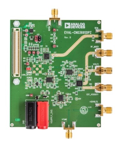
The core of this translation loop is the EVAL-CN0369-SDPZ board. Figure 6 shows a block diagram of the EVAL-CN0369- SDPZ, which uses the ADF4002 PLL, the AD8065 active loop filter, and the HMC512 VCO. The loop filter components for the active loop filter are shown in this diagram. ADIsimPLL is used to design the active loop filter.

The ADIsimPLL software is also used to design the loop filter of the translation loop PLL.
The simplest way to design a translation loop using ADIsimPLL is to replace the VCO/mixer/filter block with an equivalent VCO. If the VCO used tunes from 5.0 GHz to 5.4 GHz with KV = 150 MHz/V, and the user mixes it with a 4.9 GHz to 5.3 GHz local oscillator, the PLL sees a VCO that tunes from 400 MHz to 100 MHz with KV = 150 MHz/V.
Figure 7 shows the ADIsimPLL simulated phase noise and corresponding schematic using the ADF4002, and indicates that the PLL loop locks at 100 MHz with a minimum increase in the phase noise floor.

Translation Loop: Measured Phase Noise Results vs. Standalone PLL
Using the configuration shown in Figure 1, the f OUT rms jitter measures less than 50 fs, as shown in Table 2.
In Table 2, f REF is the reference input to the EVAL-CN0369-SDPZ from the ADF4255-2 evaluation board. The f REF provides the fine tuning for the translation loop. The local oscillator is the LO to the ADL5801-EVALZ mixer evaluation board and provides the coarse tuning for the translation loop. f OUT is the VCO/2 RF output from the EVAL-CN0369-SDPZ.
| fREF (MHz) | Local Oscillator (MHz) | fOUT Frequency (MHz) | fOUT RMS Jitter (fs) |
| 100.00 | 5300.00 | 5400.00 | 43 |
| 100.00 | 5200.00 | 5300.00 | 39 |
| 100.00 |
5100.00 | 5200.00 | 43 |
| 101.01 | 5100.00 | 5201.11 | 43 |
Figure 8 is a phase noise plot of the f OUT from the translation loop. The reference (f REF) input used in Figure 8 is 101.011 MHz to show the fine tuning performance of the translation loop. The f OUT rms jitter in Figure 8 measures less than 39 fs integrated from 1 kHz to 30 MHz.

The f OUT rms jitter measures between 200 fs and 250 fs using the ADF4355-2 as a stand-lone PLL to generate similar frequencies, as shown in Table 3.
For the Table 3 data, f REF is the low noise REFIN source for the EV-ADF4355-2SD1Z evaluation board. f OUT is the RFOUTA(+) of the EV-ADF4355-2SD1Z. RFOUTA(−) is connected to a 50 Ω terminator.
| fREF (MHz) | fOUT Frequency (MHz) | fOUT RMS Jitter (fs) |
| 100.00 | 5400.00 | 202 |
| 100.00 | 5300.00 | 220 |
| 100.00 |
5200.00 | 243 |
| 100.00 | 5201.11 | 222 |
电路评估与测试
The SDP-S board connected to the EV-ADF4355-2SD1Z board is used with the ADF4355-2 evaluation software to program the ADF4355-2 on-chip registers.
A complete set of documentation for the EVAl-CN0369-SDPZ board including schematics, layout files, and bill of materials can be found in the CN-0369 Design Support package.
Getting Started
Refer to the EVAL-CN0369-SDPZ user guide ( UG-806) for software installation and test setup.
Equipment Needed
The following equipment is needed:
- PC with a USB port and Windows® XP, Windows Vista (32-bit), or Windows 7 (32-bit)
- EVAL-CN0369-SDPZ circuit evaluation board
- EV-ADF4355-2SD1Z evaluation board
- Two EVAL-SDP-CS1Z SDP-S boards
- Integer-N v7 and the ADF4355 evaluation software
- Power supplies: 5 V, 5.5 V, and 12 V
- Two RF signal source (R&S SMA100 or equivalent)
- Spectrum analyzer (Agilent FSUP or equivalent)
- TTE 400 MHz low pass filter (or equivalent)
- Mini Circuits 100 MHz low pass filter (or equivalent)
Functional Block Diagram
See Figure 1 for the block diagram. A block diagram of the test setup is shown in Figure 9.

Setup and Test
After setting up the equipment, use standard RF test methods to measure the phase noise and phase jitter of the circuit.

样片申请及购买
样片
| 产品 |
描述 |
可提供样片的 |
| ADL5801 | 高IP3、10 MHz 至6 GHz 有源混频器 | ADL5801ACPZ-R7 |
| HMC512 | 采用SMT封装的VCO,具有Fo/2,提供4分频,9.6 - 10.8 GHz | |
| ADF4355-2 | 集成VCO的宽带频率合成器 | ADF4355-2BCPZ |
| AD8065 | 高性能、145 MHz FastFET™运算放大器 | AD8065ARTZ-REEL7 AD8065ARZ AD8065WARTZ-R7 |
| ADP151 | 超低噪声、200 mA CMOS线性调节器 | ADP151ACBZ-1.1-R7 ADP151ACBZ-1.2-R7 ADP151ACBZ-1.8-R7 ADP151ACBZ-2.75-R7 ADP151ACBZ-2.8-R7 ADP151ACBZ-3.0-R7 ADP151ACBZ-3.3-R7 ADP151ACPZ-1.5-R7 ADP151ACPZ-1.8-R7 ADP151ACPZ-2.5-R7 ADP151ACPZ-2.7-R7 ADP151ACPZ-2.8-R7 ADP151ACPZ-3.3-R7 ADP151AUJZ-1.2-R7 ADP151AUJZ-1.5-R7 ADP151AUJZ-1.8-R7 ADP151AUJZ-2.5-R7 ADP151AUJZ-2.9-R7 ADP151AUJZ-3.0-R7 ADP151AUJZ-3.3-R7 ADP151TUJZ3.3-EPR2 |
| ADM7150 | 800 mA、超低噪声/高 PSRR LDO | ADM7150ACPZ-1.8-R7 ADM7150ACPZ-3.3-R7 ADM7150ACPZ-4.5-R7 ADM7150ACPZ-4.8-R7 ADM7150ACPZ-5.0-R7 ADM7150ARDZ-1.8 ADM7150ARDZ-2.8 ADM7150ARDZ-3.0 ADM7150ARDZ-3.3 ADM7150ARDZ-5.0 |
| ADF4002 | 鉴相器/PLL频率合成器 |
- 加入我的myAnalog 登录 myAnalog