LTC4079 太阳能电池板至两节锂离子电池充电器具差分电压调节
详情介绍


概览
设计资源
设计集成文件
- Schematic
- Bill of materials
- Gerber files
- Allegro layout files
- Assembly drawing
评估硬件
产品型号带"Z"表示符合RoHS标准。评估此电路需要下列选中的电路板
- EVAL-CN0405-EB1Z ($50.00) High Voltage Output DAC with Push-Button Control
优势和特点
- High voltage DAC with push-button control
- Up to 20V output
- 64 positions
电路功能与优势
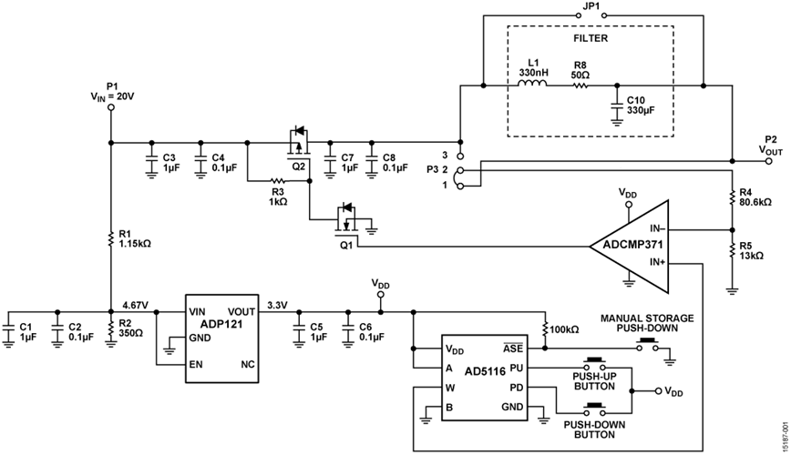
This circuit shown in Figure 1 provides a complete solution that replaces a classical high voltage mechanical potentiometer with a push-button controlled digital potentiometer.
The circuit allows a low voltage digital potentiometer to control a high voltage source up to 20 V from batteries or other sources through simple push-button switches, offering ease of use and optimum power efficiency. The AD5116 digital potentiometer provides 64 wiper positions with an end-to-end resistor tolerance error of ±8%, making it suitable for wide range of adjustment.
In addition, the AD5116 contains an EEPROM that can manually save the wiper position to its desirable position through a push-button. This feature is useful in applications requiring a default position on power-up.

电路描述
The circuit shown in Figure 1 is a simple, high voltage, variable output switching controller using the AD5116 64-position digital potentiometer in conjunction with ADCMP371 comparator that has a push-pull output stage and low power consumption suitable for battery-powered portable equipment.
The circuit is powered entirely from the VIN source and accepts an input voltage up to 20 V. The voltage from the divider, R1 and R2, is regulated to 3.3 V using the ADP121, a 30 μA, low quiescent current, low dropout linear regulator. The regulated 3.3 V supplies the VDD voltage to the AD5116 digital potentiometer and the ADCMP371 comparator.
Circuit Operation
The circuit is a switched mode power supply where the output voltage is regulated by controlling the switching frequency of the feedback network.
The output voltage, VOUT, is controlled with a feedback comparator that compares the R4 and R5 divided output voltage to a reference voltage derived from the wiper of the AD5116 digital potentiometer. The output of the comparator drives the NMOS transistor, Q1, which in turn drives the series pass PMOS transistor, Q2. The negative feedback causes Q2 to switch on and off to force the average voltage at the IN− pin of the comparator to be equal to the voltage on the IN+ pin. There is only a small amount of power dissipated in Q1 and Q2 because they are either on or off.
When the Q1 transistor is on (saturation region), the voltage drop across it is minimal, and when it is off (cutoff region), there is almost no current through the power path. The switching frequency depends on the AD5116 digital-to-analog converter (DAC) output voltage.
When the DAC output is low voltage, Q2 must be open most of the time; therefore, the comparator output must be low most of the time. Under these conditions, the comparator output is a series of short positive-going pulses at a low frequency.
As the DAC output voltage increases, Q2 must be closed for a longer period of time; therefore, the comparator output must be high longer. Under these conditions, the comparator output is a series of faster positive-going output pulses at a higher frequency. The reverse happens if the DAC output voltage is decreased.
Negative feedback forces the average value of the comparator inputs to be equal for any increase or decrease in DAC output voltage.
The filtered output voltage, VOUT, is determined by the following equation:

where VW is the DAC output voltage at the wiper terminal, W.
The AD5116 digital potentiometer generates a divided voltage at wiper to Terminal B that is proportional to the VDD voltage. The resistance between Terminal A and Terminal B is nominally 5 kΩ and is divided to 64 taps. At the lower end of the scale, the typical wiper resistance, RW, decreases to between 45 Ω and 70 Ω. The output voltage at VW with respect to GND is

where:
RWB is the wiper resistance at bottom scale.
RAB is the end-to-end resistance.
VA is the voltage at the top of the divider string, equal to VDD.
D is the decimal equivalent of the binary code in RDAC register.
The RDAC register is controlled using the PD and PU push-buttons. When a desirable wiper position is established, it can be stored to EEPROM memory through the ASE push-button, which sets the default position upon power-up.
Filtering Section
To produce a constant dc voltage and reduce the ripple voltage at the output caused by the switching that occurs at the input, an additional filtering circuit is required.
The key in determining the filter design is to determine the maximum and minimum switching frequency and define the ripple considerations, as well as the DAC operating voltage range.
The unfiltered output waveform of the circuit when the filter block is bypassed (JP1 shorted, and C10 not inserted) is shown in Figure 2 and Figure 3 for zero scale and full scale, respectively.


As shown in Figure 2 and Figure 3, the operating switching frequency of the circuit ranges from approximately 1.8 Hz (lower end of range) to 500 Hz (higher end of range). The switching ripple transients introduced onto the output waveforms can be filtered with a simple filter design that is included in the filter block section of the circuit.
The component values are dependent on the cutoff frequency of the filter. Because the switching frequencies are quite low, relatively large values of R, L, and C are required for a low cutoff frequency. However, the series resistance of the filter forms a voltage divider with the output load that can reduce the output voltage. Therefore, the value of R must be relatively small. The filter design components can be modified depending on the type of application and the load requirements.
A simple RLC low pass filter was implemented to filter the output waveform. R8 and C10 are populated with 50 Ω and 330 μF, and L1 with 100 nH for the RLC filter.
The filtered output waveform is shown in Figure 4 and Figure 5 for high voltage output and low voltage output, respectively.


The filtered outputs show that the ripple voltage is approximately 100 mV p-p. Note that the peak-to-peak ripple voltage has the same value for all codes and is not affected by the load connected to the output. The transistor used in this circuit is the IRF9630S transistor; however, it can be replaced by other transistors with the same specifications but with much lower IDSS.
Test Data and Results
The VOUT (rms) plots vs. the DAC code are shown in Figure 6 through Figure 9. These tests were conducted with an RLC filter on the output using the values shown in Figure 1 (50 Ω, 330 nH, and 330 μF).
Figure 6 shows that the output voltage is limited beyond Code 56 with no load, the point at which the comparator inputs approach the limit of their input common-mode voltage.

Figure 7 shows that the output has an error of ±5% from Code 10 to Code 54. The high percentage error in the lower codes (see Figure 6) is caused by the high offset voltage of the series side transistor, Q2.

The 50 Ω series resistor forms a voltage divider with the load. The output voltage is limited to 19.01 V with a 1 kΩ load, as shown in Figure 8.

Figure 9 shows the response with the output loaded in 1 kΩ over the linear operating range of Code 10 to Code 54.

常见变化
The performance of the circuit can be enhanced by using a pulse-width modulator (PWM) to control the on/off time ratio of the series pass transistor switching, thereby simplifying filtering. The comparator can also be replaced by an error amplifier that controls the PWM. A power transistor with low IDSS can be used to minimize ripple offset voltage at the output. A PWM controller allows greater precision in the output voltage adjustment.
The circuit can also be implemented using a buck converter with adjustable output, such as the ADP2441. The AD5116 serves as the divider that supplies the feedback pin of the buck converter. However, the output voltage must be attenuated by a factor of 4 to limit the AD5116 drive voltage to 5 V.
电路评估与测试
The circuit uses the following equipment for circuit evaluation.
Equipment Needed
The following equipment is required:
- EVAL-CN0405-EB1Z circuit evaluation board
- Agilent E36311A dual dc power supply or equivalent
- Agilent 3458A multimeter or equivalent
- Oscilloscope
Test Setup Functional Block Diagram
Figure 10 shows a functional diagram of the test setup.

Setup
Take the following steps for circuit evaluation:
- For filtered output, connect the Pin 1 and Pin 2 link of P3 with a jumper. Remove the JP1 jumper link.
- For unfiltered output, connect the Pin 2 and Pin 3 link of P3 with a jumper. Install the JP1 jumper link. Remove C10.
- Connect P2 (VOUT) to an oscilloscope/multimeter.
- Connect a 20 V supply voltage to VIN.
- Press the PU or PD button for varying output voltage.
- Press the ASE button to save a desirable output voltage upon power-up.
An Agilent E3631A supply was used to provide a 20 V input voltage. The output waveform from the EVAL-CN0405-EB1Z was captured using the oscilloscope, and the VRMS voltage was measured using the Agilent 3458A multimeter.
A complete set of documentation for the EVAL-CN0405-EB1Z board, including schematics, layouts, and bill of materials, can be found in the CN-0405 Design Support Package at www.analog.com/CN0405-DesignSupport.
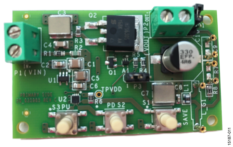
Figure 11 shows a photo of the board.

样片申请及购买
样片
| 产品 |
描述 |
可提供样片的 |
| ADP2441 | 36 V、1 A同步降压DC-DC调节器 | ADP2441ACPZ-R7 |
| ADP121 | 150 mA,低静态电流,CMOS线性稳压器,采用5引脚TSOT封装 | ADP121-AUJZ12R7 ADP121-AUJZ15R7 ADP121-AUJZ18R7 ADP121-AUJZ25R7 ADP121-AUJZ28R7 ADP121-AUJZ30R7 ADP121-AUJZ33R7 |
| ADCMP371 | 推挽输出级的通用型比较器 | ADCMP371-KGD-RL7 ADCMP371AKSZ-REEL7 |
| AD5116 | 单通道、64位、按钮式、±8%电阻容差、非易失性数字电位计 | AD5116BCPZ10-500R7 AD5116BCPZ80-500R7 |
- 加入我的myAnalog 登录 myAnalog